


Device Applications
Keithley 6517B instrument can also be used for measuring the parameters for Solar cell and Diodes in darkness and under illumination through I-V characteristics.
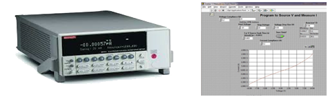 Keithley 6517B electrometer/High resistance meter of solar cell and diode measurements
1. Solar cell
A solar cell is an electronic device, which directly converts sunlight into electricity. Light shining on the solar cell produces both a current and a voltage to generate electric power. This process requires firstly, a material in which the absorption of light raises an electron to a higher energy state, and secondly, the movement of this higher energy electron from the solar cell into an external circuit. The electron then dissipates its energy in the external circuit and returns to the solar cell. A variety of materials and processes can potentially satisfy the requirements for photovoltaic energy conversion, but in practice nearly all photovoltaic energy conversion uses semiconductor materials in the form of a p-n junction.
The basic steps in the operation of a solar cell are:
- the generation of light-generated carriers;
- the collection of the light-generated carriers to generate a current;
- the generation of a large voltage across the solar cell; and
- the dissipation of power in the load and in parasitic resistances.
Uniformly and fully fabricated solar cell device is required for characterization.
2. Diodes
A diode is a unidirectional device permitting the easy current flow in one direction but resisting the flow in opposite direction.
If an external potential is applied to the terminals of a PN junction, it will alter the potential between the P and N-regions. This potential difference can alter the flow of majority carriers, so that the PN junction can provide an opportunity for the diffusion of electrons and holes. If the voltage applied decreases the width of the depletion layer, then the diode is assumed to be in the forward bias and if the applied voltage increases the depletion layer width then the diode is assumed to be in the reverse bias mode. If the width of depletion layer does not alter then it is in the zero bias state.
Applications of P-N Junction Diodes
- As rectifier in DC Power Supplies.
- In Demodulation or Detector Circuits.
- In clamping networks used as DC Restorers
- In clipping circuits used for waveform generation.
- As switches in digital logic circuits.
Uniformly and fully fabricated diode device is required for characterization.